(Applied Physical Chemistry)

(Applied Physical Chemistry)
(b.1964), B.S.(1987,Waseda), Ph.D.(1992, Waseda), Res.Assoc.(1991, Waseda), Assist.Prof. (1993, Waseda), Assoc.Prof.(1996, Waseda), Prof.(2005, Waseda). Visiting Assoc.Prof.(1997, Stanford). Principle Investigator, NSF I/UC Research Center for Silicon Wafer Engineering and Defect Sciences.
Shibata Memorial Award, Surface Finishing Society of Japan (1991), Ando Incentive Prize for the Stidy of Electronics (1997), Sano Award for Young Scientists, Electrochemical Society of Japan (1999), Award for Young Scientists, Surface Finishing Society of Japan (1999). International Union of Surface Finishing (UK), INTERFINISH Best Paper Award (2000), The Electrochemical Society Research Award (Electrodeposition Division) (2010).
keywords
Functional Surface Chemistry / Electrochemistry / Silicon Wet Device Processes / Scanning Probe Microscopy / Data Storage Devices
Room 65-200
3-4-1 Okubo, Shinjuku-ku, Tokyo 169-8555, Japan
Tel: +81-3-5286-3209
Fax: +81-3-3205-2074
E-mail:t.homma@waseda.jp
Research Interests
The surface of materials possess unique characteristics which potentially may lead to novel functional properties. Our research is directed towards creating nanostructured surfaces and thin films with novel functions at solid-liquid interfaces, evaluating their microstructural and functional properties in nanometer scale, and also analyzing surface reactions in silicon wet device processes, from the view point of physical chemistry.
Our current research involves creating thin films and nanostructured surfaces with novel electronic or magnetic functions, ex-situ and in-situ analyses of their deposition processes and deposition reaction mechanism, performing computer simulation of these processes, developing new methods for evaluating structural and functional properties of the nanostructured surfaces in nanometer scale mainly by scanning probe microscopy (SPM: such as scanning tunneling microscopy (STM), atomic force microscopy (AFM), scanning surface potential microscopy (SPoM), tunneling AFM (TAFM), magnetic force microscopy (MFM)), and applying such surfaces to the development of devices and systems such as high-sensitive sensing devices for X-ray imaging and immunoassay, electrochemical micro reactors, high-density data storage system, as well as atomistic and electrochemical understanding of silicon surface chemistry under device processing conditions.
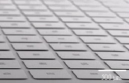
Fig. SEM image of the microabsorber array for X-Ray imaging sensor device
fabricated by the electrodeposition process.
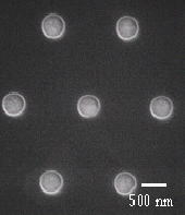
Fig. SEM images for the patterned magnetic nanodots formed by electroless
deposition process.
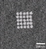
Fig. Representative TMAFM image of Cu nano dot array electrochemically fabricated on the silicon wafer surface.
Selected Publications
(1)“Density Functional Theory Analysis of Reaction Mechanism of Hypophosphite Ions on Metal Surfaces,” J. Electrochem. Soc., 158, D585-D589 (2011).
(2)“Density Functional Theory Analysis for Orbital Interaction between Hypophosphite Ions and Metal Surfaces,” J. Electrochem. Soc., 158, D626-D633 (2011).
(3)“CoNiP Electroless Deposition Process for Fabricating Ferromagnetic Nanodot Arrays,” Electrochim. Acta 56, 9575-9580 (2011).
(4)“Electrochemical Etching Process to Tune the Diameter of Arrayed Deep Pores by Controlling Carrier Collection at a Semiconductor-Electrolyte Interface,” Electrochem. Comm, 12, 765-768 (2010).
(5)“Transient Mass Transfer Rate of Cu2+ Ion Caused by Copper Electrodeposition with Alternating Electrolytic Current,” Electrochim. Acta, 55, 3987-3994 (2010).
(6)“Synchrotron Radiation-induced Total Reflection X-ray Fluorescence Analysis,” Trends in Analytical Chemistry, 29, 479-496 (2010).
(7)“Fabrication of Magnetic Nanodot Array using Electrochemical Deposition Processes,” Electrochim. Acta, 55, 8081-8086 (2010).
(8)“Raman Microscopy and Scanning Surface Potential Microscopy Analysis of Nanoscale Defects on Si Wafer Surfaces” , J. Electrochem. Soc., 156, H475-H478 (2009).
(9)“Effect of Cu Seed Layers on the Properties of Electroplated Sn-Cu Films”, J. Electrochem. Soc., 156, E86-E90 (2009).
(10)“Fabrication of Catalyst-Functionalized Three Dimensional Micromesh Structures”, Jpn. J. Appl. Phys., 47, 5204-5207 (2008).
(11)“Characterization of the Surface Layer on Strained Si Wafer by Electrochemical Methods”, J. Phys. Chem. C, 112, 3785-3788 (2008).
(12)“Estimation of Redox Potential of Strained Si by Density Functional Theory Calculation”, J. Phys. Chem. C, 112, 3104-3107 (2008).
Back to: